

MINGJIAN IMAGING
Reimagining advanced packaging inspection with computational optics
High-precision 3D imaging for online semiconductor packaging inspection across CoWoS, BGA, C4 and SIP.
About Mingjian Imaging
MINGJIAN IMAGING
High-precision 3D imaging for online semiconductor packaging inspection across CoWoS, BGA, C4 and SIP.
About Mingjian ImagingCORE PRODUCTS
High-precision 3D and synchronized 3D + 2D optical metrology for advanced packaging and precision electronics.

High-performance 3D optical metrology module
A 3D inspection solution for PCBs, semiconductor packages and precision electronic structures, balancing measurement accuracy with inline production speed.

Synchronized 3D + 2D optical metrology module
Built for die-bond, wire-bond and SIP inspection, delivering synchronized 3D + 2D measurement for advanced packaging, micro-assembly, high-speed optical modules and lead frames.
ABOUT MINGJIAN
Mingjian Imaging supplies 3D imaging modules for complete online inspection of semiconductor packaging, delivering high-performance, high-precision and stable solutions for inspection and metrology equipment makers.
Learn moreImprove CoWoS process yield and build the foundation for AI computing.
Stay committed to independent innovation and customer-first growth.
Build full-chain 3D imaging modules around advanced packaging needs.
Set a new standard for complete online 3D inspection of semiconductor packaging.
APPLICATIONS
Four verified inspection applications spanning micro-assembly, lead frames, micro solder paste, PCBA and BGA.

Capture clear images of reflective dies and first/second bond points while measuring aluminium-wire arc height and die glue height.
Learn more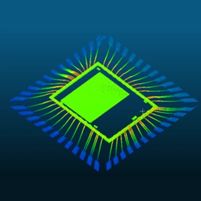
Synchronously present 3D height and 2D grayscale results for lead-frame CMOS sensors and 800G optical-module optoelectronic chips.
Learn more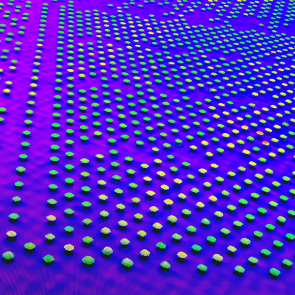
Designed for advanced packaging applications such as CoWoS, this solution performs 3D topography and cross-sectional profile measurement of microbumps on wafer surfaces, delivering synchronized 3D height and 2D grayscale outputs.
Learn more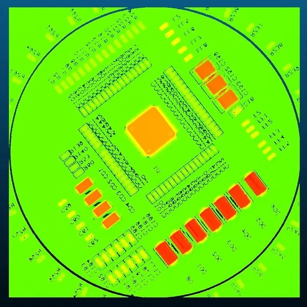
Inspect PCBA chips, resistors, capacitors and BGA solder balls with 3D maps, 2D height maps and profile sections.
Learn moreOUR TEAM / CHIP COLLABORATION
Align chips, algorithms and software on one map so every decision can be verified.

The R&D team discussing a chip solution
NEWSROOM

Mingjian Imaging will showcase its advanced-packaging inspection capabilities at the 2026 IICIE International Integrated Circuit Innovation Expo.
Read more
Mingjian Imaging will present advanced-packaging inspection solutions at the 2026 Bay Area Semiconductor Industry Ecosystem Expo.
Read moreVISION
Advance semiconductor packaging quality control through high-speed, high-precision inline inspection.
Contact


